

Taiwan Semiconductor Manufacturing Company debuted its next-generation A13 process technology at the in Santa Clara, California, on Wednesday, positioning the new node as the foundation for AI accelerators, high-performance computing systems, and mobile chips entering the market in 2029 and beyond. The announcement came as part of a broader update that also previewed an A12 variant with backside power delivery, a refreshed 2nm platform called N2U, and the first 14-reticle Chip on Wafer on Substrate packaging for AI systems.
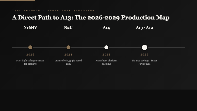
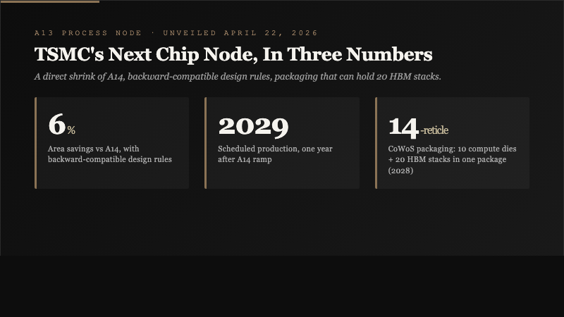
A13 is not a ground-up node. It is a direct shrink of the A14 platform TSMC announced in 2025, engineered to keep design rules fully backward-compatible so customers can migrate existing A14 designs with minimal rework. The shrink delivers 6 percent area savings, measurable power efficiency improvements, and a density bump driven by design-technology co-optimization on the company's nanosheet transistor architecture. Production is scheduled to begin in 2029, one year after A14.
Why a "Direct Shrink" Matters in 2026
In semiconductor manufacturing, a direct shrink of an existing node is less glamorous than a completely new process, but it is often more commercially important. The shrink preserves the design kit that chip designers have already built their tooling around, which collapses the engineering calendar for migrating a product from the older node to the new one. For customers building AI accelerators on 24-month development cycles, that compatibility is the difference between shipping a product in the generation it was designed for and missing the window entirely.
The 6 percent area savings translates, in practice, into either a smaller and cheaper die for a given transistor count, or a meaningfully larger transistor budget at the same die area. For AI chip designers, the second option is usually the one that matters. More transistors inside a power envelope mean more systolic array cells, larger on-chip SRAM blocks, or higher HBM interconnect density. All three are binding constraints on the generation of AI accelerators that will ship in 2029 and 2030.
"At TSMC, we understand our customers are always looking ahead to their next innovation and they come to us for a reliable stream of new silicon technologies, like A13, meticulously engineered to be ready for high-volume production right when their visionary new designs demand them."
C.C. Wei, Chairman and CEO, TSMC
The theme of the North America Technology Symposium, "Expanding AI with Leadership Silicon," is not a coincidence. Every technology layer TSMC disclosed during the event is tuned specifically for the design constraints of AI training and inference hardware.
The Other Shoe: A12, N2U, and the Broader Roadmap
TSMC disclosed several additional technologies at the event that fill out the 2026 through 2029 production roadmap for customers that include NVIDIA, AMD, Apple, Broadcom, and a growing list of hyperscaler-designed custom silicon programs.
| Node / Technology | Production Timing | Key Characteristic |
|---|---|---|
| N2U (2nm refresh) | 2028 | 3-4% speed gain or 8-10% power reduction vs N2P, 1.02-1.03x density |
| A14 | 2028 | Base nanosheet platform announced 2025 |
| A12 (A14 enhancement) | 2029 | Super Power Rail backside power delivery for AI/HPC |
| A13 (A14 shrink) | 2029 | 6% area savings, design-rule backward compatible |
| N2A (automotive) | AEC-Q100 qualification 2028 | First nanosheet automotive-grade process |
| N16HV (high voltage) | 2026 | First FinFET high-voltage process for displays |
The A12 variant is the more architecturally significant of the new node announcements. It adds Super Power Rail technology, TSMC's branding for backside power delivery, which routes power through the back side of the wafer rather than through the same metal stack used for signal routing. Intel's PowerVia implementation of a similar concept has shown measurable improvements in voltage droop and signal integrity at advanced nodes. A12 brings that capability to TSMC's customer base for AI and HPC designs entering production in 2029.
On the 2nm platform, N2U uses design-technology co-optimization to reach 3 to 4 percent speed gains or 8 to 10 percent power reduction compared to N2P, with a 1.02 to 1.03x logic density improvement. For designers targeting the transition window between today's 3nm production and the 2028 ramp of N2U, the node is meant to be a drop-in upgrade path rather than a ground-up redesign.
The Packaging Story Is Half the Performance
The A13 announcement dominated headlines, but the more immediately commercially important news from the symposium was in advanced packaging. TSMC is already producing 5.5-reticle Chip on Wafer on Substrate packages, and the company disclosed that a 14-reticle CoWoS capable of integrating approximately 10 large compute dies and 20 HBM stacks is slated for production in 2028. The size bump after that, scheduled for 2029, is expected to push beyond 14 reticles.
For customers like NVIDIA, the CoWoS roadmap matters as much as or more than the logic node itself. The current generation of AI training accelerators is already memory-bound for many large-model workloads, and a package that can accommodate 20 HBM stacks inside the same reticle field expands the addressable memory bandwidth substantially without requiring a new system architecture.
TSMC also disclosed that its TSMC-SoIC 3D chip stacking technology will be available with A14-to-A14 stacks in 2029, providing 1.8x higher die-to-die input/output density compared with current N2-on-N2 SoIC. And the company said its TSMC-COUPE on-substrate co-packaged optics solution will begin production in 2026, with a 200Gbps micro-ring modulator that TSMC claims delivers 2x power efficiency and 10x latency reduction versus pluggable optics.
Without ASML's Next-Gen Tool
A detail worth surfacing from TSMC's announcement is what it did not say. The A13 roadmap does not require the next generation of ASML's extreme ultraviolet lithography tool, the High-NA EUV system that lithography watchers expected to be a gating factor for post-A14 nodes. Reuters, in reporting on the symposium, noted that TSMC is showing a path to smaller and faster chips without dependency on the tool that ASML has been ramping for delivery to Intel, Samsung, and competing fabs.
The technical implementation involves more aggressive use of design-technology co-optimization, double patterning techniques on existing low-numerical-aperture EUV scanners, and tighter process integration between the logic layer and backside power delivery. The business implication is that TSMC's capital equipment runway for the A13 and A12 generations is shorter and cheaper than it would be if High-NA were mandatory, and TSMC's customers get a cost curve that does not rely on a tool whose yield and throughput have not yet been demonstrated at production scale.
"The direct shrink is a classic TSMC play. They give customers a migration path that does not require redesign, they bank the process maturity from the prior node, and they slide a cost reduction into the road map without needing the most expensive tool in the industry."
Industry analyst comments cited in Reuters coverage of the symposium, April 22, 2026
Automotive and Specialty Nodes
Beyond the AI-focused disclosures, TSMC announced N2A, its first automotive-grade process technology built on nanosheet transistors. N2A delivers a 15 to 20 percent speed gain at the same power compared with N3A, TSMC's current automotive-grade 3nm process. The node is scheduled to complete AEC-Q100 qualification, the industry-standard reliability testing requirement for automotive semiconductors, in 2028.
For automakers and Tier 1 suppliers designing the next generation of ADAS and autonomous vehicle compute platforms, N2A is an important signal that leading-edge process technology will be available on the automotive reliability calendar rather than lagging commercial nodes by two generations. More than 10 products are already planned on N3A for production in 2026, following TSMC's "Auto Early" program that let customers begin designs in 2023.
The company also announced N16HV, which TSMC is billing as the first high-voltage process in the FinFET era. For smartphone display drivers, N16HV increases gate density by 41 percent and reduces power by 35 percent compared to the company's existing N28HV process. For near-eye displays used in AR and smart glasses applications, the new process can shrink die area by 40 percent and cut power by more than 20 percent.
What to Watch Going Into 2027 and 2028
TSMC's disclosures set the pace for the rest of the foundry industry. Samsung and Intel, both of which are investing heavily in advanced logic capacity, now have to match or beat TSMC's 2028 N2U production schedule and 2029 A12/A13 ramp with their own nodes. Samsung's SF2 process and Intel's 18A are the closest competitors on the timeline, and both have taken longer to yield at production volumes than their original roadmaps projected.
For customers designing AI training hardware for 2029 availability, the decision point is roughly this: commit to A14 or A12 at TSMC with the shrink path to A13, or bet on a competing foundry whose node may deliver comparable performance but with higher execution risk. The 2026 symposium made the TSMC option look lower-risk, which is why the announcement moved sentiment for TSMC's AI-exposed customer base.
For related coverage, see our reporting on NVIDIA's Vera Rubin roadmap and trillion-dollar backlog, on Google's Marvell-partnered custom AI chip program, and on the Broadcom, Google, and Anthropic custom AI chip deal structure.
Sources
- TSMC Debuts A13 Technology at 2026 North America Technology Symposium - TSMC Press Release
- TSMC shows smaller, faster chips without a pricey new tool from ASML - Reuters
- TSMC Debuts A13 Technology at 2026 North America Technology Symposium - TechPowerUp
- TSMC Debuts A13: The Next Engine of AI and Mobile Innovation - CommonWealth Magazine


